
Summary: Scanning electron microscopy and energy spectrum testing were used to study the copper protective layers of two different printed circuit boards, namely Organic Solderability Preservatives (OSP) and Immersion Ag (I-Ag), for lead-free solder joints. The impact of the structure. The results show that the thickness of the intermetallic compound layer at the soldering interface using the organic protective layer is significantly higher than that of the immersion silver layer; in the solder joints of the two different protective layers, flaky or dendritic Ag3 Sn intermetallic compounds are present, but in the dip In the silver layer solder joints, the flaky Ag3 Sn mainly grows non-uniformly at the interface layer of the solder, while in the solder joint of the organic protective layer, the flaky Ag3 Sn is less likely to be formed, and the dendritic Ag3 Sn is uniformly distributed. In the solder joints. Fracture analysis showed that there were more pores in the solder joints with organic protective layer, and the pores mainly appeared in the copper joints, which significantly reduced the strength of the solder joints.
With the approach of the European Union in July 2006 that all electronic and electrical products entering the market must meet the lead-free legal deadline, the lead-free process of electronic products is receiving more and more attention from manufacturers. Although many studies have shown that lead-free assembly is feasible and has some favorable features, there are still many problems to be solved before the electronic assembly industry fully implements lead-free. The important point is how to ensure better printing. The circuit board is effectively compatible with lead-free alloys. From the viewpoint of electronic properties, Sn-Ag-Cu is considered to be a promising alloy system for replacing eutectic Sn-Pb, which has good wettability on copper surface and can form good solder joints. Its thermal performance also exceeds the eutectic Sn-Pb alloy. To ensure with Sn - Ag
- Cu maintains good wetting characteristics during assembly. It is necessary to surface-treat the copper surface of the printed circuit board before assembly by adding a protective layer such as an organic protective layer (OSP) or a immersion silver layer ( Im2mersion Ag, I - Ag), immersion gold layer (Immersion Au, I - Au), electroless Ni/Au layer, etc., which are mostly used for organic protective layer and immersion silver layer, and the two protective layer pairs are used. Research on the influence of lead-free solder joint structure has not been reported yet. To this end, combined with the lead-free surface mount technology process in actual production, the influence of the copper surface protection layer of printed circuit board on the structure of lead-free Sn-Ag-Cu solder joints was studied.
1 Experimental process <br> Using a lead-free solder paste with an alloy composition of Sn - 3. 0 % Ag - 0. 5 % Cu (mass percent), flux for rosin The BGA component is soldered according to the surface mount technology process, that is, the vacuum printed printed circuit board is unsealed, the solder paste template is printed, and the reflow soldering furnace is used. The copper side of the printed circuit board uses two different protective layers, an organic protective layer and a immersion silver layer. The holding zone temperature during reflow is 218 °C and the peak temperature is 235 °C. After reflow soldering, a series of lead-free BGA / Cu solder samples were prepared. The BGA was separated from the printed circuit board by the tensile test method, and then the change of the solder joint breakage and the fracture was observed under a scanning electron microscope to determine the influence of the copper protective layer on the fracture mode of the solder joint. The tensile rate was 0. . 5 mm / min. To determine the effect of the copper protective layer on the solder joint structure, the BGA /Cu solder sample is cut at the same position on the printed circuit board. After polishing, φ (HNO3 ) 5 % +φ (HCl) 2 % +φ is used. H2O2) 0. 5 % mixed acid solution for corrosion treatment, and then micro-etched with a volume fraction of 25% nitric acid solution. For the different weld samples after corrosion treatment, the JEOLJSM6360 scanning electron microscope (SEM) with INCA EDS was used for observation and analysis.
2 test results and analysis <br> Lead-free solder joints protected by organic protective layer After the tensile test, a large number of solder joints break near the copper surface as shown in Fig. 1 (a), showing that the strength of the lead-free solder joint is lower than that of the copper surface. The bonding strength of the printed circuit board; the fracture point of the broken solder joint shows that there are more air holes in the solder joint as shown in Fig. 1 (b), and the pore sizes are different, and the flux has flux residue. After the tensile test of the lead-free solder joint protected by the immersion silver layer, most of the copper surface is pulled out as shown in Fig. 1 (c), which shows that the strength of the solder joint is higher than the joint strength of the copper surface and the printed circuit board; The fractured joint observation shows that the fracture is relatively flat, as shown in Figure 1 (d).
There are fewer stomata.
The main reason for the occurrence of pores in the solder joint of the organic protective layer is that the organic protective layer is decomposed and generated by the reflow furnace, and these gases form pores near the interface because they are not ready to be discharged. When the solder joint is subjected to an external force, stress concentration occurs at the air hole and microcracks are formed, and the micro crack then expands and grows, and finally causes the solder joint to break, thereby reducing the strength of the solder joint.
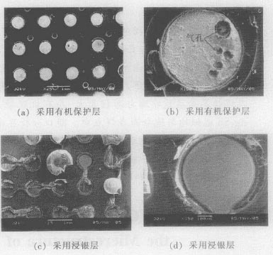
Figure 1 Scanning electron microscopy analysis of fractures of lead-free solder joints after tensile test
The welding samples of different protective layers were etched back and the tin alloy covered on the copper surface was etched away. The SEM observation showed that the morphology of the pebbles was as shown in Fig. 2. The energy spectrum test showed that the particles were Cu6 Sn5 phase. This is similar to lead soldering. However, the statistical analysis shows that the average diameter of the Cu6 Sn5 phase particles in the solder joint is 2.696 μm, which is 30% higher than the average diameter of the particles in the immersion silver layer (average 1.945 μm).
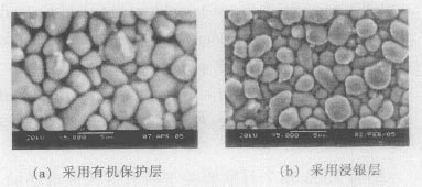
Figure 2 Cu6 Sn5 phase morphology on the copper surface
After the solder joint slicing test, scanning electron microscopy analysis showed that there were flaky or dendritic Ag3 Sn in the solder joints as shown in Fig. 3. The flaky Ag3 Sn mainly grows on the solder interface layer, but a large amount of flaky Ag3 Sn appears on the solder interface layer as shown in Fig. 3 (c) and Fig. 3 (d). This indicates that Ag3 Sn is more prone to non-uniform nucleation growth on the immersion silver-protected solder interface layer. The energy spectrum analysis showed that the solder interface layer consisted of intermetallic compound (IMC) Cu6 Sn5 phase and Cu3 Sn. The thickness of the solder interface layer with organic protective layer was 10μm, which was significantly higher than that of the immersion silver layer (average 5μm). . In addition, the analysis also showed that there were pores on the welded interface of the organic protective layer as shown in Fig. 3 (a) and Fig. 3 (b), which further confirmed the results of the fracture observation.
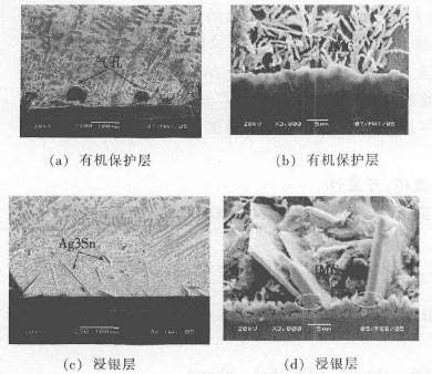
Figure 3 Scanning electron micrograph of solder joint slice structure
After the printed circuit board passes through the reflow oven, the organic protective layer is decomposed under the action of high temperature, and the tin-silver-copper alloy melts and reacts with the copper surface to form Cu6 Sn5. As the reaction progresses, Cu and tin on the copper surface The Sn in the silver-copper alloy further interdiffused, so that the chemical composition of the Cu6 Sn5 phase near the copper surface changes and eventually forms the Cu3 Sn phase, and the Cu6 Sn5 phase near the solder joint end further grows. When the protective layer is a immersion silver layer, due to the blocking effect of Ag, the interdiffusion speed of Sn in the Cu surface and the tin-silver-copper alloy on the copper surface is reduced, the Cu6 Sn5 phase length is reduced, and the thickness of the interface layer is also increased. Correspondingly; in addition, since the Ag on the copper surface melts and adheres to some Cu6 Sn5 phase when passing through the reflow oven, the Cu6 Sn5 phase containing Ag on the surface becomes a non-uniform nucleation point, with the reaction The Cu in the non-uniform nucleation point is outwardly diffused, and Ag and Sn in the solder joint diffuse toward the nucleation point in the solder joint, and finally the Ag3 Sn phase is formed and further grown as shown in FIG. 3(d). As for the growth of Ag3 Sn, the growth of the Ag3 Sn phase may be due to the specific habit of the Ag3 Sn phase. These habits have the characteristics of low nucleation energy and are easy to grow Ag3 Sn along the habit.
3 Conclusion <br> The copper surface protection of printed circuit boards has an impact on the structure of lead-free solder joints. The size and number of pores in the lead-free solder joints using the organic protective layer are significantly larger than those in the immersion silver layer. The solder joints protected by the organic protective layer are mainly broken near the copper surface. The interface analysis showed that the thickness of the solder interface layer protected by the organic layer exceeded the solder joint of the immersion silver layer. The welded interface using the immersion silver layer has a large amount of flaky Ag3 Sn intermetallic compound which grows in the form of flakes.
With the approach of the European Union in July 2006 that all electronic and electrical products entering the market must meet the lead-free legal deadline, the lead-free process of electronic products is receiving more and more attention from manufacturers. Although many studies have shown that lead-free assembly is feasible and has some favorable features, there are still many problems to be solved before the electronic assembly industry fully implements lead-free. The important point is how to ensure better printing. The circuit board is effectively compatible with lead-free alloys. From the viewpoint of electronic properties, Sn-Ag-Cu is considered to be a promising alloy system for replacing eutectic Sn-Pb, which has good wettability on copper surface and can form good solder joints. Its thermal performance also exceeds the eutectic Sn-Pb alloy. To ensure with Sn - Ag
- Cu maintains good wetting characteristics during assembly. It is necessary to surface-treat the copper surface of the printed circuit board before assembly by adding a protective layer such as an organic protective layer (OSP) or a immersion silver layer ( Im2mersion Ag, I - Ag), immersion gold layer (Immersion Au, I - Au), electroless Ni/Au layer, etc., which are mostly used for organic protective layer and immersion silver layer, and the two protective layer pairs are used. Research on the influence of lead-free solder joint structure has not been reported yet. To this end, combined with the lead-free surface mount technology process in actual production, the influence of the copper surface protection layer of printed circuit board on the structure of lead-free Sn-Ag-Cu solder joints was studied.
1 Experimental process <br> Using a lead-free solder paste with an alloy composition of Sn - 3. 0 % Ag - 0. 5 % Cu (mass percent), flux for rosin The BGA component is soldered according to the surface mount technology process, that is, the vacuum printed printed circuit board is unsealed, the solder paste template is printed, and the reflow soldering furnace is used. The copper side of the printed circuit board uses two different protective layers, an organic protective layer and a immersion silver layer. The holding zone temperature during reflow is 218 °C and the peak temperature is 235 °C. After reflow soldering, a series of lead-free BGA / Cu solder samples were prepared. The BGA was separated from the printed circuit board by the tensile test method, and then the change of the solder joint breakage and the fracture was observed under a scanning electron microscope to determine the influence of the copper protective layer on the fracture mode of the solder joint. The tensile rate was 0. . 5 mm / min. To determine the effect of the copper protective layer on the solder joint structure, the BGA /Cu solder sample is cut at the same position on the printed circuit board. After polishing, φ (HNO3 ) 5 % +φ (HCl) 2 % +φ is used. H2O2) 0. 5 % mixed acid solution for corrosion treatment, and then micro-etched with a volume fraction of 25% nitric acid solution. For the different weld samples after corrosion treatment, the JEOLJSM6360 scanning electron microscope (SEM) with INCA EDS was used for observation and analysis.
2 test results and analysis <br> Lead-free solder joints protected by organic protective layer After the tensile test, a large number of solder joints break near the copper surface as shown in Fig. 1 (a), showing that the strength of the lead-free solder joint is lower than that of the copper surface. The bonding strength of the printed circuit board; the fracture point of the broken solder joint shows that there are more air holes in the solder joint as shown in Fig. 1 (b), and the pore sizes are different, and the flux has flux residue. After the tensile test of the lead-free solder joint protected by the immersion silver layer, most of the copper surface is pulled out as shown in Fig. 1 (c), which shows that the strength of the solder joint is higher than the joint strength of the copper surface and the printed circuit board; The fractured joint observation shows that the fracture is relatively flat, as shown in Figure 1 (d).
There are fewer stomata.
The main reason for the occurrence of pores in the solder joint of the organic protective layer is that the organic protective layer is decomposed and generated by the reflow furnace, and these gases form pores near the interface because they are not ready to be discharged. When the solder joint is subjected to an external force, stress concentration occurs at the air hole and microcracks are formed, and the micro crack then expands and grows, and finally causes the solder joint to break, thereby reducing the strength of the solder joint.
The welding samples of different protective layers were etched back and the tin alloy covered on the copper surface was etched away. The SEM observation showed that the morphology of the pebbles was as shown in Fig. 2. The energy spectrum test showed that the particles were Cu6 Sn5 phase. This is similar to lead soldering. However, the statistical analysis shows that the average diameter of the Cu6 Sn5 phase particles in the solder joint is 2.696 μm, which is 30% higher than the average diameter of the particles in the immersion silver layer (average 1.945 μm).
After the solder joint slicing test, scanning electron microscopy analysis showed that there were flaky or dendritic Ag3 Sn in the solder joints as shown in Fig. 3. The flaky Ag3 Sn mainly grows on the solder interface layer, but a large amount of flaky Ag3 Sn appears on the solder interface layer as shown in Fig. 3 (c) and Fig. 3 (d). This indicates that Ag3 Sn is more prone to non-uniform nucleation growth on the immersion silver-protected solder interface layer. The energy spectrum analysis showed that the solder interface layer consisted of intermetallic compound (IMC) Cu6 Sn5 phase and Cu3 Sn. The thickness of the solder interface layer with organic protective layer was 10μm, which was significantly higher than that of the immersion silver layer (average 5μm). . In addition, the analysis also showed that there were pores on the welded interface of the organic protective layer as shown in Fig. 3 (a) and Fig. 3 (b), which further confirmed the results of the fracture observation.
After the printed circuit board passes through the reflow oven, the organic protective layer is decomposed under the action of high temperature, and the tin-silver-copper alloy melts and reacts with the copper surface to form Cu6 Sn5. As the reaction progresses, Cu and tin on the copper surface The Sn in the silver-copper alloy further interdiffused, so that the chemical composition of the Cu6 Sn5 phase near the copper surface changes and eventually forms the Cu3 Sn phase, and the Cu6 Sn5 phase near the solder joint end further grows. When the protective layer is a immersion silver layer, due to the blocking effect of Ag, the interdiffusion speed of Sn in the Cu surface and the tin-silver-copper alloy on the copper surface is reduced, the Cu6 Sn5 phase length is reduced, and the thickness of the interface layer is also increased. Correspondingly; in addition, since the Ag on the copper surface melts and adheres to some Cu6 Sn5 phase when passing through the reflow oven, the Cu6 Sn5 phase containing Ag on the surface becomes a non-uniform nucleation point, with the reaction The Cu in the non-uniform nucleation point is outwardly diffused, and Ag and Sn in the solder joint diffuse toward the nucleation point in the solder joint, and finally the Ag3 Sn phase is formed and further grown as shown in FIG. 3(d). As for the growth of Ag3 Sn, the growth of the Ag3 Sn phase may be due to the specific habit of the Ag3 Sn phase. These habits have the characteristics of low nucleation energy and are easy to grow Ag3 Sn along the habit.
3 Conclusion <br> The copper surface protection of printed circuit boards has an impact on the structure of lead-free solder joints. The size and number of pores in the lead-free solder joints using the organic protective layer are significantly larger than those in the immersion silver layer. The solder joints protected by the organic protective layer are mainly broken near the copper surface. The interface analysis showed that the thickness of the solder interface layer protected by the organic layer exceeded the solder joint of the immersion silver layer. The welded interface using the immersion silver layer has a large amount of flaky Ag3 Sn intermetallic compound which grows in the form of flakes.
WN Flanges Connect Pipe,Carbon Steel Flanged Fittings,Stainless Steel Flanged Concentric Reducer,Pipe Flange Connection
Cangzhou Youlong Pipe Fitting Manufacturing Co., LTD , https://www.ypco88.com